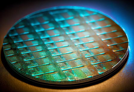
Scientists have devised a breakthrough in developing Silicon Wafers by making them as thick as an atom with a 12-inch diameter, Boasting higher capability than currently in-use wafers.
The new material has superior semiconducting properties, and the researchers believe it has the potential to revolutionize the silicon chip industry. Although more work is required to convert this 2D material into viable chips, this breakthrough is a significant step forward.
As silicon wafers become thinner, their voltage control improves, resulting in more heat generation and higher energy costs when turned into chips. Naturally, this presents a challenge in producing as small as possible semiconductors.
Manufacturing 12-inch Silicon wafers with materials an atom thick is, of course, challenging. Scientists struggle to keep the layers uniform as the wafer's diameter increases. Although two-inch wafers have been successfully produced in the past, 12-inch wafers now account for roughly 60% of the chip market. Any 2D material would need to be scaled up to be compatible with existing machinery and designs.
To address the size issue, the team abandoned traditional point-to-surface methods in favor of what it calls a surface-to-surface supply method. The researchers then created their apparatus to support the new method.
According to Liu, the team can now produce 10,000 2D wafers per machine per year. Notably, Liu mentions that the method can produce wafers larger than 12 inches if necessary. The new surface-to-surface process represents a significant advancement, allowing for precise and efficient manufacturing.
We use cookies to ensure you get the best experience on our website. Read more...